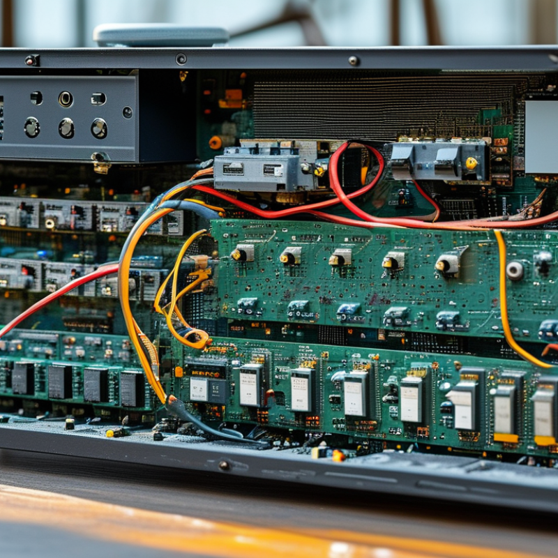
| PCB Functional Sections | Common sections include power conversion, battery charging, DC protection, AC switching, control logic, sensing, communication, and auxiliary power. | The PCB coordinates power flow between photovoltaic panels, batteries, household loads, and the utility grid. | Confirm that the board architecture supports the required operating modes: grid-tied, battery backup, off-grid, and solar priority. | Check connectors, relays, fuses, terminal blocks, and communication interfaces for discoloration, looseness, corrosion, or heat damage. |
| System Power Rating | Residential hybrid inverter systems commonly range from approximately 3 kW to 15 kW; larger commercial systems may be rated above 15 kW. | The PCB must carry the expected current without excessive temperature rise or electrical stress. | Match the PCB design with the inverter's continuous power, short-term overload capability, battery voltage, and maximum PV input power. | Inspect high-current paths for darkened copper, lifted pads, cracked solder joints, and abnormal heating during operation. |
| Battery Voltage Range | Typical battery buses include approximately 48 V for low-voltage battery systems and approximately 100–600 V for high-voltage battery systems. | Battery voltage determines insulation requirements, switching-device ratings, sensing accuracy, and protection design. | Verify compatibility with the battery chemistry, nominal voltage, maximum charge voltage, discharge limits, battery management system, and communication protocol. | Keep battery terminals tight and dry. Never work on the PCB while the battery and PV sources are energized. |
| Maximum DC Input Voltage | Many residential PV inputs are designed for several hundred volts DC. The exact limit depends on the inverter design and local installation conditions. | Excessive DC voltage can damage switching devices, capacitors, insulation, and measurement circuits. | Select a PCB whose voltage rating exceeds the calculated maximum cold-weather open-circuit voltage of the PV strings. | Check for insulation breakdown, carbon tracking, damaged surge components, and loose PV connectors after abnormal events or lightning. |
| Maximum PV Input Current | A typical residential MPPT input may support roughly 10–30 A per tracker, but the permitted value varies by inverter model and design. | Input-current limits protect PCB traces, fuses, inductors, connectors, and semiconductor switches from overload. | Compare the short-circuit current and operating current of each PV string with the PCB and inverter input limits, including applicable design margins. | Inspect DC terminals, current sensors, fuses, and inductors for hot spots or signs of sustained overcurrent. |
| MPPT Performance | Modern solar inverters commonly use one or more independent maximum power point trackers to accommodate different roof orientations and shading conditions. | Stable MPPT control improves energy harvest when irradiance and module voltage change throughout the day. | Consider the number of MPPT channels, MPPT voltage window, startup voltage, maximum current per tracker, and independent string support. | Review operating data for abnormal voltage fluctuations, repeated tracking faults, or a sudden drop in energy yield from one channel. |
| Switching Devices | Power PCBs may use MOSFETs, IGBTs, or other semiconductor switches selected according to the DC voltage, current, switching frequency, and topology. | Switching devices control conversion efficiency, thermal performance, noise, overload response, and long-term reliability. | Check voltage and current ratings, switching losses, thermal resistance, gate-drive compatibility, and the availability of qualified replacement parts. | Maintain clean heat-transfer surfaces and verify that fans, heat sinks, thermal pads, and temperature sensors operate correctly. |
| Capacitor Selection | DC-link and filtering circuits may use electrolytic, film, or ceramic capacitors. Lifetime is strongly affected by temperature, ripple current, and voltage stress. | Capacitors stabilize the DC bus, reduce ripple, and support reliable switching. Degradation can cause increased ripple, alarms, and converter failure. | Check capacitance, voltage rating, ripple-current rating, temperature rating, expected service life, and the capacitor's physical fit on the PCB. | Look for bulging, leakage, venting, discoloration, elevated ripple, or unusual acoustic noise. Replace only with parts meeting the original specifications. |
| Thermal Design | Electronic component life generally decreases as operating temperature rises. A commonly used engineering rule is that a 10°C increase can approximately double the reaction rate of many aging processes. | Effective heat dissipation limits semiconductor, capacitor, relay, and solder-joint stress. | Evaluate heat sinks, airflow paths, thermal sensors, fan control, enclosure ventilation, and the inverter's permitted ambient temperature range. | Keep ventilation openings clear, remove dust with approved methods, and record temperature alarms or repeated thermal derating. |
| PCB Materials and Construction | Power boards commonly use multilayer constructions with copper thickness selected according to current, temperature rise, and mechanical requirements. | Suitable materials improve insulation strength, current capacity, mechanical stability, and resistance to thermal cycling. | Review board thickness, copper weight, creepage and clearance, solder mask quality, conformal coating requirements, and thermal-via design. | Inspect for delamination, cracked solder joints, moisture residue, damaged coating, and contamination around high-voltage areas. |
| Electrical Protection | Common protection devices include fuses, circuit breakers, surge protective devices, pre-charge circuits, overvoltage protection, and overtemperature shutdown. | Protection reduces damage caused by short circuits, switching surges, lightning-induced transients, and abnormal operating conditions. | Confirm protective-device ratings, interruption capacity, coordination, grounding arrangement, and compatibility with the installation voltage. | Check protective indicators, replace operated fuses with the correct type, and investigate the cause before re-energizing the system. |
| Isolation and Safety Spacing | Required creepage, clearance, insulation, and dielectric withstand values depend on working voltage, pollution level, altitude, and applicable safety standards. | Adequate isolation helps prevent arcing, electric shock, fire, and control-side damage between high-voltage and low-voltage circuits. | Use a PCB evaluated for the target voltage and environment, with clearly separated power, control, communication, and protective-earth paths. | Do not bridge, scrape, drill, or modify isolation barriers. Test insulation only with procedures approved for the specific inverter. |
| Communication Interfaces | Common interfaces include CAN, RS-485, Ethernet, Wi-Fi, and dry-contact or digital-input connections. | Communication enables battery state reporting, remote monitoring, energy management, firmware updates, and coordinated shutdown. | Confirm protocol compatibility, isolation, connector type, cable length, termination requirements, and cybersecurity provisions. | Check communication cables, shielding, termination resistors, connectors, error logs, and firmware status without interrupting approved safety controls. |
| Environmental Protection | Outdoor inverter enclosures are commonly specified with an ingress-protection rating such as IP65 or a comparable level, depending on the product design. | Protection from dust, moisture, condensation, and salt mist helps prevent corrosion, leakage current, and insulation failure. | Match the PCB coating and enclosure protection to the installation location, humidity, pollution level, altitude, and coastal or agricultural conditions. | Inspect enclosure seals, cable glands, drain paths, condensation, corrosion, and signs of insects or water entry. |
| Efficiency and Standby Consumption | Well-designed solar inverters often achieve peak conversion efficiencies above 95%, while actual daily efficiency varies with load, temperature, battery operation, and operating mode. | Lower conversion losses reduce heat generation and improve usable solar and battery energy. | Compare efficiency curves rather than relying only on peak efficiency. Consider MPPT efficiency, battery charge/discharge efficiency, and standby use. | Compare long-term energy data with expected site conditions and investigate unexplained increases in nighttime or standby consumption. |
| Quality and Testing | Relevant evaluation commonly includes functional testing, thermal testing, insulation testing, electromagnetic-compatibility testing, and protection verification. | Testing reduces the risk of latent defects and verifies that the PCB performs safely under normal and abnormal conditions. | Request traceable test records, incoming inspection criteria, burn-in or load-test procedures, and documented revision control. | Keep maintenance records containing fault codes, test results, component replacements, firmware revisions, and inspection dates. |
| Recommended Maintenance Interval | Visual and environmental checks are commonly performed at least annually; dusty, humid, coastal, or high-temperature sites may require more frequent inspections. | Routine maintenance identifies airflow restrictions, loose connections, corrosion, and abnormal heating before major failure occurs. | Set the interval according to the manufacturer's service instructions, site conditions, operating hours, and local electrical regulations. | Isolate AC, PV, and battery energy sources using the approved shutdown procedure, then allow stored energy to discharge before qualified servicing. |
| Replacement and Repair Decision | A PCB should be repaired or replaced when it has repeated faults, burned conductors, damaged isolation barriers, failed protection circuits, or components that cannot be safely verified. | Correct decisions reduce downtime and prevent secondary damage to batteries, PV modules, loads, and grid-connected equipment. | Use a form-fit-function compatible board with matching hardware, firmware, ratings, connectors, protection features, and revision requirements. | Repairs should be performed only by qualified personnel using ESD controls, approved test equipment, and documented commissioning checks. |
| Key Selection Priorities | Electrical compatibility, thermal capability, environmental durability, safety protection, communication support, serviceability, and lifecycle cost. | A PCB that matches the complete system is more important than one selected only by nominal power rating or initial purchase price. | Use a technical checklist covering voltage, current, MPPT, battery interface, protection, cooling, standards, monitoring, warranty, and spare parts. | Reassess performance after major system changes, including battery expansion, PV-string modification, firmware updates, or changes in operating environment. |